• Skip to primary navigation
  • Skip to main content
  • Skip to footer
Prior Scientific

Prior Scientific

Experts in Precision Positioning and Microscope Automation

  • Products
    • Automated Imaging Systems
      • OpenStand-U
      • OpenStand-M
      • OpenStand-L
      • OpenStand-V
    • Imaging Components
      • Motorized Stages
      • Focus Mechanisms
      • Laser Autofocus
      • Filter Wheels, Turrets & Shutters
      • Controllers & Joysticks
      • Robotic Sample Loaders
      • Physiology Platforms
      • Motorized Vertical Stages
    • Microscope Automation
      • Evident Olympus Microscope Automation
      • Nikon Microscope Automation
      • Leica Microscope Automation
      • Zeiss Microscope Automation
      • Automated Custom Imaging Systems
      • Other Microscope Brands
    • Nanopositioning Devices
    • Vibration Control
    • Custom Solutions & Contract Manufacturing
  • About
  • Applications
  • Blog
  • Contact Us
  • News
  • Technical Support
  • US Shop
  • United States
    • English
    • Deutsch
    • 日本語
    • 简体中文
  • Automated Imaging Systems
    • OpenStand-L
    • OpenStand-M
    • OpenStand-U
    • OpenStand-V
  • Imaging Components
    • Motorized Stages
    • Focus Mechanisms
    • Laser Autofocus
    • Filter Wheels, Turrets & Shutters
    • Controllers & Joysticks
    • Robotic Sample Loaders
    • Physiology Platforms
    • Motorized Vertical Stages
  • Microscope Automation
    • Evident Olympus Microscope Automation
    • Nikon Microscope Automation
    • Leica Microscope Automation
    • Zeiss Microscope Automation
    • Automated Custom Imaging Systems
    • Other Microscope Brands
  • Nanopositioning Devices
  • Vibration Control
  • Custom Solutions & Contract Manufacturing
Home » Applications » Automated Imaging for Semiconductor Inspection

Automated Imaging for Semiconductor Inspection

Increasing throughput and ensuring quality with high-speed, high-precision positioning and autofocus

Semiconductor inspection requires extreme precision and reliability because the slightest imperfections can affect chip performance. 

With wafer features measured at the nanometer scale, inspection systems must deliver sub-micron accuracy, consistent repeatability, and stable positioning.

Advanced imaging, combined with vibration control, is essential for effectively detecting imperfections. Automating these processes not only enhances accuracy but also improves efficiency, reducing human error, and increasing throughput for high-volume manufacturing.

A wide range of imaging modalities may be used. Some examples and applications are:

Detecting surface defects: 
•    Bright field and darkfield microscopy
•    Atomic force microscopy 
•    Confocal microscopy 

Examining the internal structure of the wafers:
•    Infrared microscopy
•    SWIR (Short Wave Infrared) imaging

Challenges for semiconductor inspection

Precise imaging of wafers at the nanometer scale, without compromising speed

While the detail of a semiconductor wafer is small, the wafers themselves are large – up to 300 mm (12 inches) in diameter. The imaging system must be able to move the sample quickly to cover the entire area, while offering sub-nanometer resolution. 

Weight is another challenge. For imaging, wafers are often mounted in carriers, cassettes, vacuum chucks, or environmental enclosures that add additional weight. For high-resolution imaging, some equipment – such as heavy objectives – may be mounted directly on the stage. The combined weight is often several kilograms. 

Prior Scientific Solution:

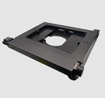
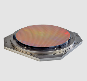
ProScan H112 Motorized Stage with Queensgate WP120A Single Axis Wafer Piezo Stage

The WP120A piezo wafer stage from Queensgate holds 300 mm wafers, has a Z-axis travel range of 120 µm, with 5.5 nm repeatability. It is compatible with the H112 large-format motorized stage from Prior, which has 302 mm XY travel. The H112 features a 2 mm ballscrew for speed, together with Intelligent Scanning Technology (IST) for enhanced linearity and accuracy. 

High-load, high-accuracy piezo z-stages from Queensgate

The NPS-X-60D, NPS-X-100D, and NPS-Z-250B are high-load nanopositioning piezo stages. When configured for vertical travel (Z-axis), they precisely position and hold the heavy optical assemblies used for semiconductor inspection.  

Flexure guidance and low-noise capacitive sensors ensure precise positioning and stability. Learn more about Queensgate’s solutions for semiconductor and hard disk inspection.

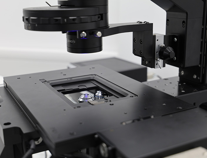
OpenStand-L: Large Format Microscopy Platform

Because each semiconductor fab is unique, a complete, customized inspection system is often required. The OpenStand-L is modular and compatible with Prior’s large-format motorized stages and other components; Queensgate’s piezo nanopositioning stages; and a host of third-party integrations are possible. 

Maintain sharp focus across the wafer surface

Silicon wafers aren’t perfectly flat and may have thickness variations, both within the wafer and due to raised features in the patterning. Imaging systems will need to refocus continually during the inspection, which can slow down the entire process.

Prior Scientific Solution:

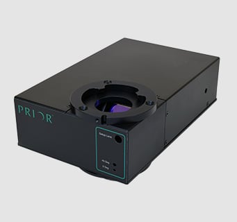
PureFocus850 and PureFocus690 Laser Autofocus Systems

PureFocus adjusts in real time to uneven surfaces or inconsistent reflectivity – such as the surface of a silicon wafer. PureFocus’ line mode ensures stability for industrial samples by averaging the focus across the field of view.

It uses interface detection recognition to target the correct surface when the sample has multiple reflective layers, which eliminates time-consuming recalibrations. 

CASE STUDY: Rapid scanning of Silicon Carbide wafers using Prior Scientific’s PureFocus 850 Autofocus

Environmental factors can compromise measurement stability

The inspection is often carried out under carefully controlled conditions – such as in a vacuum – to eliminate contaminants and reduce optical distortion. Temperature changes affect materials, so it's important to select nanopositioning products with low thermal expansion. Effective vibration control is also essential. 

Prior Scientific Solution:

Many Queensgate nanopositioning piezo stages are designed to operate in UHV conditions. Both the Queensgate NPS-XYP-250Q 300 mm Wafer Mask Alignment Stage and WP120A wafer stage operate in high vacuum and have low thermal expansion properties, making them suitable for a wide range of semiconductor applications. 

Passive vibration control workstations and optical tables. 

Kinetic Systems offers vibration control for automation and testing equipment. As well as off-the-shelf workstations and control platforms, they work with customers to develop custom products for specific applications in the semiconductor industry. 

Enquire Now
Colourful image of etched silicon wafers reflecting patterns of light.

Related Products

H112/2ST Large Format Motorized XY Stage

ProScan H112/2ST Large Format Motorized XY Stage

Piezo z-axis stage for semiconductor inspection with a 12-inch silicon wafer.

WP120A 12-inch Single Axis Wafer Piezo Stage

PureFocus690 hardware laser autofocus system on a grey background.

PureFocus™690 Laser Autofocus System

View All Products

Articles

Close up of a motorized xy stage on an OpenStand-V inverted imaging platform. imaging platform
7/27/2026

Microscopy and Precision Positioning Glossary: Terms, Definitions and Industry Guide

↘ View Article
H100A compact precision motorized XY stage for upright microscopes
6/15/2026

H100A Compact Motorized XY Microscope Stage for Precision Microscopy: Product Manager Q&A

↘ View Article
Three quarters view of the Prior motorized filter cube turret for multi-colour fluorescence imaging.
5/13/2026

How a motorized filter cube turret expands microscope performance across advanced imaging workflows

↘ View Article
4/21/2026

HF108B Filter Wheel: High‑Speed Fluorescence Imaging for Automated Microscopy Systems

↘ View Article
View Articles

Footer

Products

  • Automated Imaging Systems
  • Imaging Components
  • Microscope Automation
  • Nanopositioning Devices

Company

  • Custom Solutions & Contract Manufacturing
  • Applications
  • Technical Support
  • Careers

Resources

  • About
  • Blog
  • News
  • Contact Us

    Sign up to stay in the know...

    ✉

    Connect with us

    Prior Scientific Instruments Ltd.
    Units 3-4 Fielding Industrial Estate
    Wilbraham Road, Fulbourn
    Cambridge, CB21 5ET, UK

    inquiries@prior.com
    +44 (0)1223 881711

    Prior Scientific Inc.
    80 Reservoir Park Drive
    Rockland, MA. 02370
    U.S.A.

    info@prior.com
    +1 781 878 8442

    Prior Scientific Instruments GmbH
    Maria-Pawlowna-Str. 4
    07743 Jena
    Germany

    jena@prior.com
    +49 (0)3641 242 010

    Prior Scientific KK
    Kayabacho 3rd Nagaoka Bldg 10F,
    2-7-10, Nihonbashi Kayabacho
    Chuo-Ku, Tokyo 103-0025, Japan

    info-japan@prior.com
    +81 (0)3 5652 8831

    Prior Scientific Instruments (Suzhou) Ltd.
    Room 118, Meilihua Hemu Park,
    No. 393 Suhong Middle Road,
    Suzhou Industrial Park,
    Suzhou, 215000, China

    info-china@prior.com
    +86 (0)512 6617 5866

    Copyright © 2026 · Prior Scientific. Terms & Conditions | Privacy Policy | Impressum

    Manage Consent
    To provide the best experiences, we use technologies like cookies to store and/or access device information. Consenting to these technologies will allow us to process data such as browsing behavior or unique IDs on this site. Not consenting or withdrawing consent, may adversely affect certain features and functions.
    Functional Always active
    The technical storage or access is strictly necessary for the legitimate purpose of enabling the use of a specific service explicitly requested by the subscriber or user, or for the sole purpose of carrying out the transmission of a communication over an electronic communications network.
    Preferences
    The technical storage or access is necessary for the legitimate purpose of storing preferences that are not requested by the subscriber or user.
    Statistics
    The technical storage or access that is used exclusively for statistical purposes. The technical storage or access that is used exclusively for anonymous statistical purposes. Without a subpoena, voluntary compliance on the part of your Internet Service Provider, or additional records from a third party, information stored or retrieved for this purpose alone cannot usually be used to identify you.
    Marketing
    The technical storage or access is required to create user profiles to send advertising, or to track the user on a website or across several websites for similar marketing purposes.
    • Manage options
    • Manage services
    • Manage {vendor_count} vendors
    • Read more about these purposes
    View preferences
    • {title}
    • {title}
    • {title}